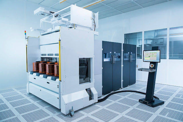
Increasing Demand for Consumer Electronics to Boost Growth of the Wafer Inspection Equipment Market
Wafer manufacturing is an electrical process
that consists of several repetitive, step-by-step processes to form complete
photonic or electrical circuits on thin, transparent semiconductor wafer
materials. Examples include the manufacture of LEDs, radio frequency generators,
photo-resistors, microprocessors, and other electronics.
Wafer inspection equipment is used to detect
defects during wafer manufacturing processes. These equipment detect both the
pattern defects and the physical defects by obtaining the coordinates of the
defect’s position. Inspection equipment improve the quality of manufactured
semiconductor device. Therefore, these inspection devices are indispensable for
maintaining the production yield of semiconductors.
Market
Dynamics:
Increasing demand for high performing and low
cost semiconductors is expected to augment the growth of the wafer inspection equipment market. For instance,
in May 2020, TCS launched TCS WaferWise, a cloud-based wafer anomaly detection
solution that harnesses the company’s contextual knowledge of the semiconductor
industry and power of deep learning technology, to help chip makers digitally
reimagine their product quality assurance process.
Moreover, increasing demand for inspection
equipment, the increasing demand for consumer electronics and the increasing
need for high-quality electronic components is expected to propel growth of the
wafer inspection equipment market. For instance, in September 2020, KLA
launched an enhanced portfolio of inspection systems, which include the Kronos
1190 wafer-level packaging inspection system, the ICOS F160XP die sorting and
inspection system, and the ICOS T3/T7 Series of packaged IC component
inspection and metrology systems.
Furthermore, the Internet of Things (IoT) and
digitization are major trends in the market, which will require semiconductor
technologies as the basis of their framework. Vehicle automation, kitchen
automation, smart connected TVs, smart grids, smart city, are among the many
IoT concepts expected to gain traction in the next few years.
Competitive
Analysis:
Major players operating in the wafer
inspection equipment market are Toray Engineering, Rudolph Technologies, Tokyo
Seimitsu, Planar Corporation, Nanometrics, Nikon, Lam Research, Lasec
Corporation, JEOL, Hitachi High-Technologies, KLA-Tencor, FEI (Thermo Fisher
Scientific), Hermes Microvision (ASML), Zeiss Global, and Applied Materials.
In January 2021, CyberOptics Corporation
announced that the company will showcase the WX3000 metrology and inspection
system with Multi-Reflection Suppression (MRS) sensor technology, and
high-precision sensors for semiconductor tool set-up and diagnostics at the
Virtual SEMI Technology Unites Global Summit in February 2020.
In December 2018, ISRA VISION launched an
inspection system that allows wafer edges to be monitored during the entire
manufacturing process.
In July 2018, KLA-Tencor announced two new
defect-inspection products, addressing key challenges in tool and process
monitoring during silicon wafer and chip manufacturing at the leading-edge
logic and memory nodes.


Comments
Post a Comment